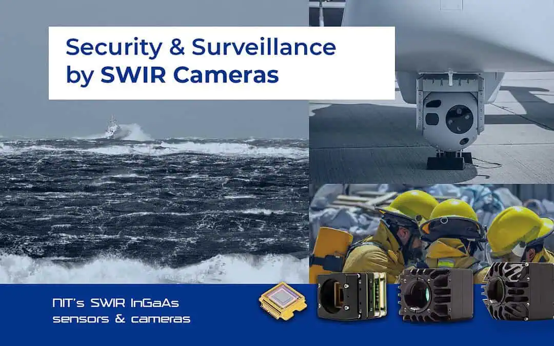
Enhance Security and Surveillance with NIT SWIR InGaAs Cameras
The need for advanced imaging technology is critical in the ever-evolving landscape of security and surveillance. NIT’s comprehensive range of SWIR (Short-Wave Infrared) InGaAs sensors and cameras delivers superior performance, offering unmatched clarity in challenging environments. Whether it’s for perimeter security, critical infrastructure monitoring, or tactical defense operations, NIT’s solutions excel in demanding applications.
Why SWIR Cameras for Security and Surveillance?
SWIR cameras provide a unique advantage in security and surveillance, thanks to their ability to “see” through challenging conditions such as haze, rain, or darkness, where conventional visible cameras fail. They can also penetrate obscurants like smoke, pollution or snow, delivering clear, actionable images. This makes them essential for border security, critical site monitoring, and tactical situational awareness.
Moreover, SWIR cameras enable enhanced detail detection due to their ability to capture high-contrast imagery in harsh conditions without the need for additional lighting. This offers the ability to detect hidden objects, identify individuals, and monitor activity in environments that are otherwise invisible to standard cameras.
Related content:
NIT’s Advanced SWIR Camera Solutions for Security and Surveillance
NIT offers a broad range of SWIR cameras designed specifically for security and surveillance, incorporating industry-leading features:
-
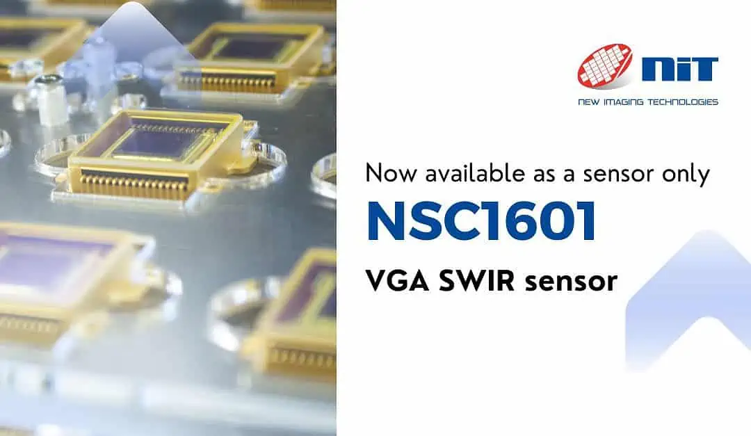
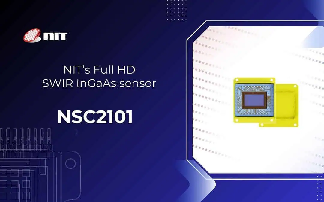
NSC1601 Sensor:
High Sensitivity and HDR: NIT’s VGA-resolution NSC1601 InGaAs sensor offers an industry-leading high dynamic range (HDR) of up to 120dB, capturing detailed images across a wide range of lighting conditions. Its high sensitivity makes it ideal for detecting small objects or people at great distances, even under low-light conditions.
-
Modular and Versatile Cameras:
NIT manufactures board-level modules and complete SWIR cameras with multiple interface options, including USB 3.0 and SDI, allowing for flexible integration into existing surveillance systems.
-
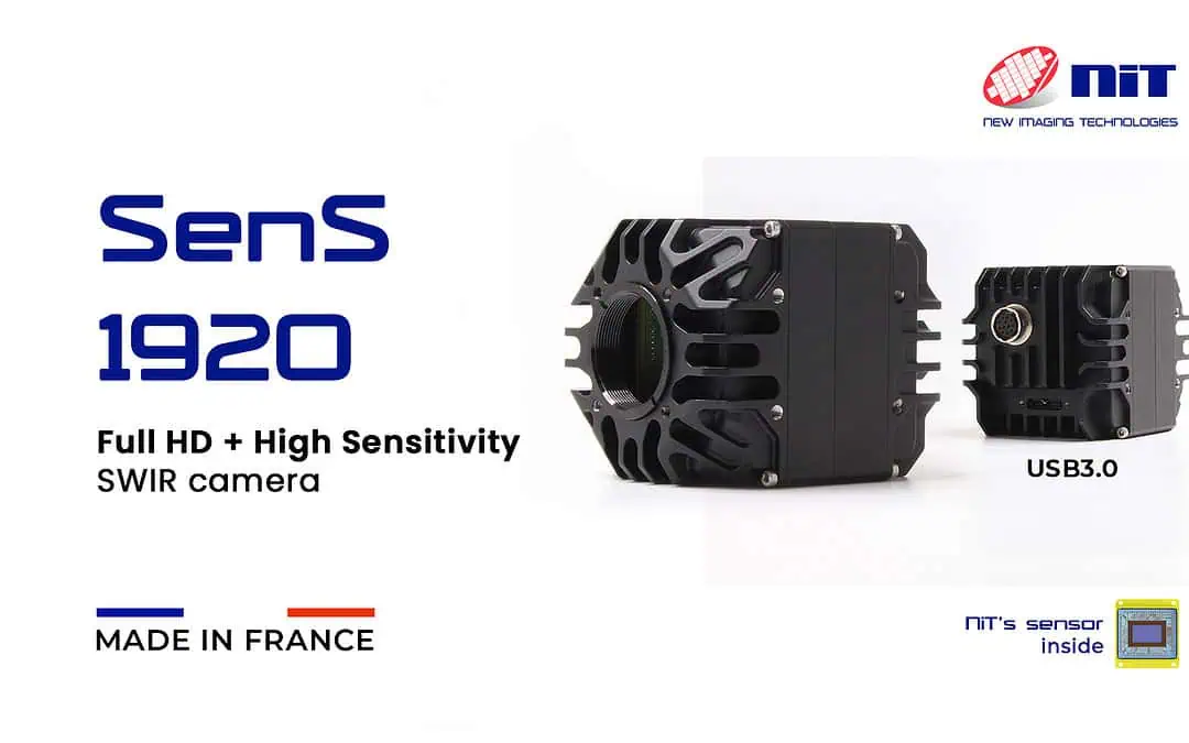
Full HD Resolution and Ultra-Low Noise:
NIT’s SWIR cameras, such as the SenS 1920, offer high resolution up to Full HD (1920×1080 pixels) and provide unmatched detail and clarity. Coupled with ultra-low noise performance (down to 25e-), these cameras ensure superior image quality, allowing for accurate monitoring and threat detection even in extreme environments.
-
Gated Imaging Technology:
NIT SWIR cameras come equipped with gated imaging, a powerful feature that enhances the ability to see through obstructions like dust or smoke. This capability is essential in situations requiring heightened situational awareness, such as law enforcement operations or border patrol, where every detail matters.
-
Long-Range Observation with Zoom Capability:
NIT’s SWIR cameras are ideal for long-range surveillance, especially when equipped with motorized zoom optics. SWIR wavelengths are less affected by atmospheric conditions, enabling clear observation of distant objects. With the addition of zoom functionality, operators can focus on targets miles away while maintaining sharp image quality, making these cameras perfect for perimeter security, border patrol, and military applications requiring detailed, long-distance monitoring.
Key Benefits of NIT SWIR Cameras for Security and Surveillance
- Unmatched Performance in Challenging Environments: Whether monitoring in complete darkness or through obscurants like fog and smoke, NIT’s SWIR cameras deliver clear, high-quality images.
- Enhanced Threat Detection: With high resolution up to Full HD and ultra-low noise, NIT cameras provide the detailed imagery needed to identify potential threats from a distance.
- Flexible Integration: NIT offers multiple camera models with a range of interfaces and configurations, allowing easy integration into existing security infrastructure.
- Proven Reliability: NIT designs and manufactures its own SWIR sensors and cameras, ensuring full control over quality and performance. Our cameras are built to withstand the toughest environments while delivering consistent high-performance results.
Applications of SWIR Cameras in Security and Surveillance
- Perimeter Security: Detect intruders and breaches in real-time
- Critical Infrastructure Monitoring: Protect power plants, airports, and other sensitive locations from unauthorized access or sabotage.
- Tactical Defense: Equip military and law enforcement with high-performance imaging for enhanced situational awareness during missions.
- Border Security and Long-Range Observation: Monitor vast border areas and distant targets under various environmental conditions, ensuring safety and security over large distances.
With NIT’s state-of-the-art SWIR InGaAs cameras, security professionals can achieve greater visibility, sharper images, and enhanced situational awareness. Our solutions are designed to give you the edge when it matters most.
Explore NIT’s range of SWIR solutions for your security and surveillance needs today!
SWIR imaging solutions
Contact NIT today for more information about our SWIR imaging solutions for security and surveillance application.