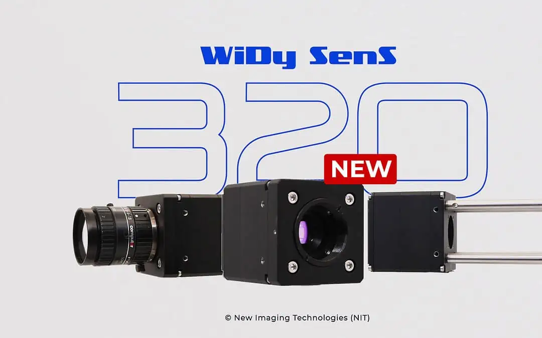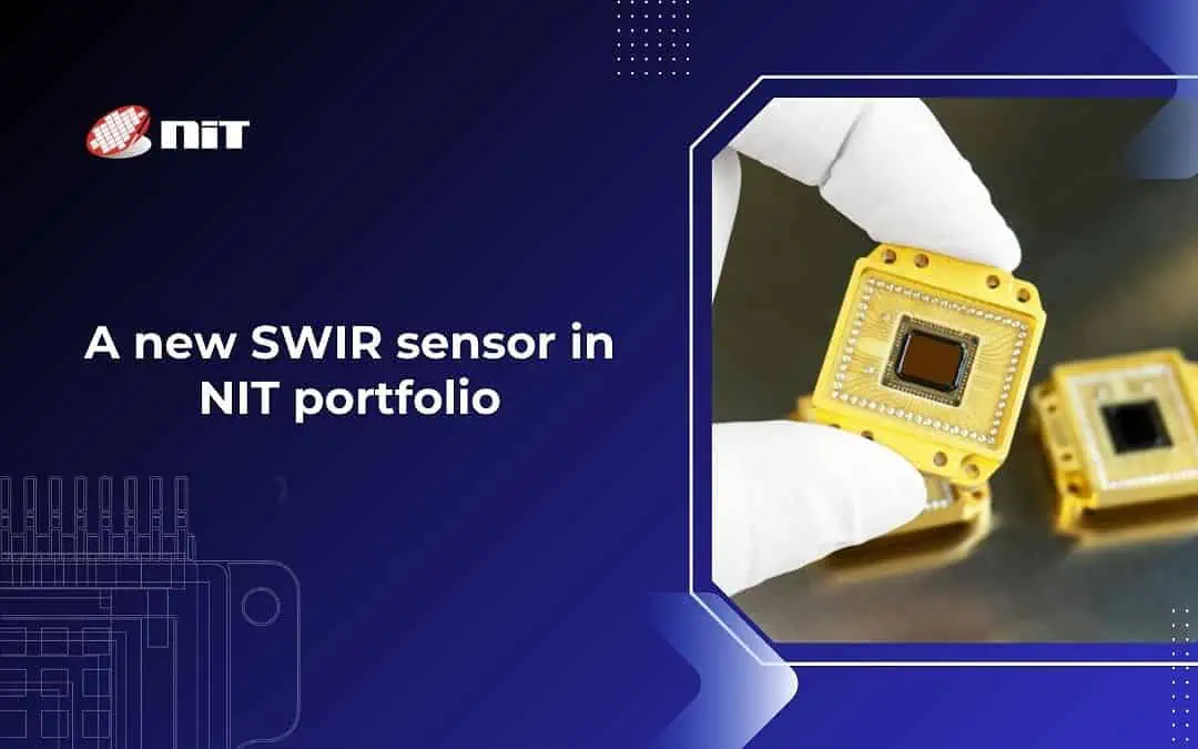
New High-Resolution, SWIR Sensor with High Performance
Overview
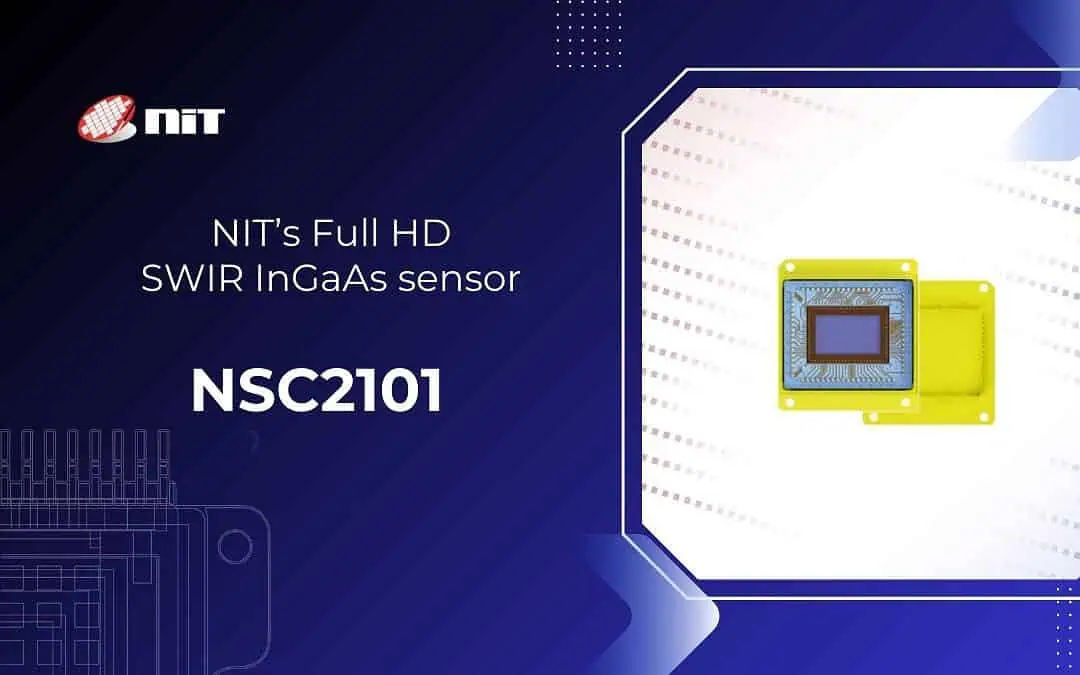
The new SWIR sensor – NSC2101 boasts remarkable features, including a high-performance InGaAs sensor with an 8µm pixel pitch, delivering an impressive 2MPIX resolution at 1920x1080px. Its ultra-low noise of only 25e- ensures exceptional image clarity, even in challenging environments. Additionally, with a dynamic range of 64dB, the sensor captures a wide spectrum of light intensities with precision and accuracy.
- 0.9µm to 1.7µm spectrum
- 2MPix – 1920x1080px @8µm pixel pitch
- 25e- readout noise
- 64dB dynamic range
This cutting-edge sensor is designed and manufactured by NIT in France and promises unparalleled performance and reliability. Leveraging advanced technology and expertise, NIT has crafted a sensor that meets the rigorous standards of ISR applications, offering crucial insights and intelligence in various scenarios.
Image example


Applications
The applications of this SWIR sensor are vast and diverse, catering to the needs of defense, security, and surveillance industries. The sensor’s capabilities are indispensable for enhancing situational awareness and decision-making, from monitoring border security to providing critical intelligence in tactical operations.
Typical applications:
- Intelligence, Surveillance, and Reconnaissance (ISR)
- Semiconductor, wafer, solar panel inspection
Extension
Moreover, NIT’s commitment to innovation extends beyond the sensor itself. The camera version, integrating the NSC2101 sensor, will be released soon.
Full HD SWIR sensor