Semiconductor inspection
Semiconductor Inspection with SWIR Imaging: Detect Hidden Defects in Silicon
Semiconductor manufacturing requires detecting defects and structures that are often invisible with conventional imaging technologies.
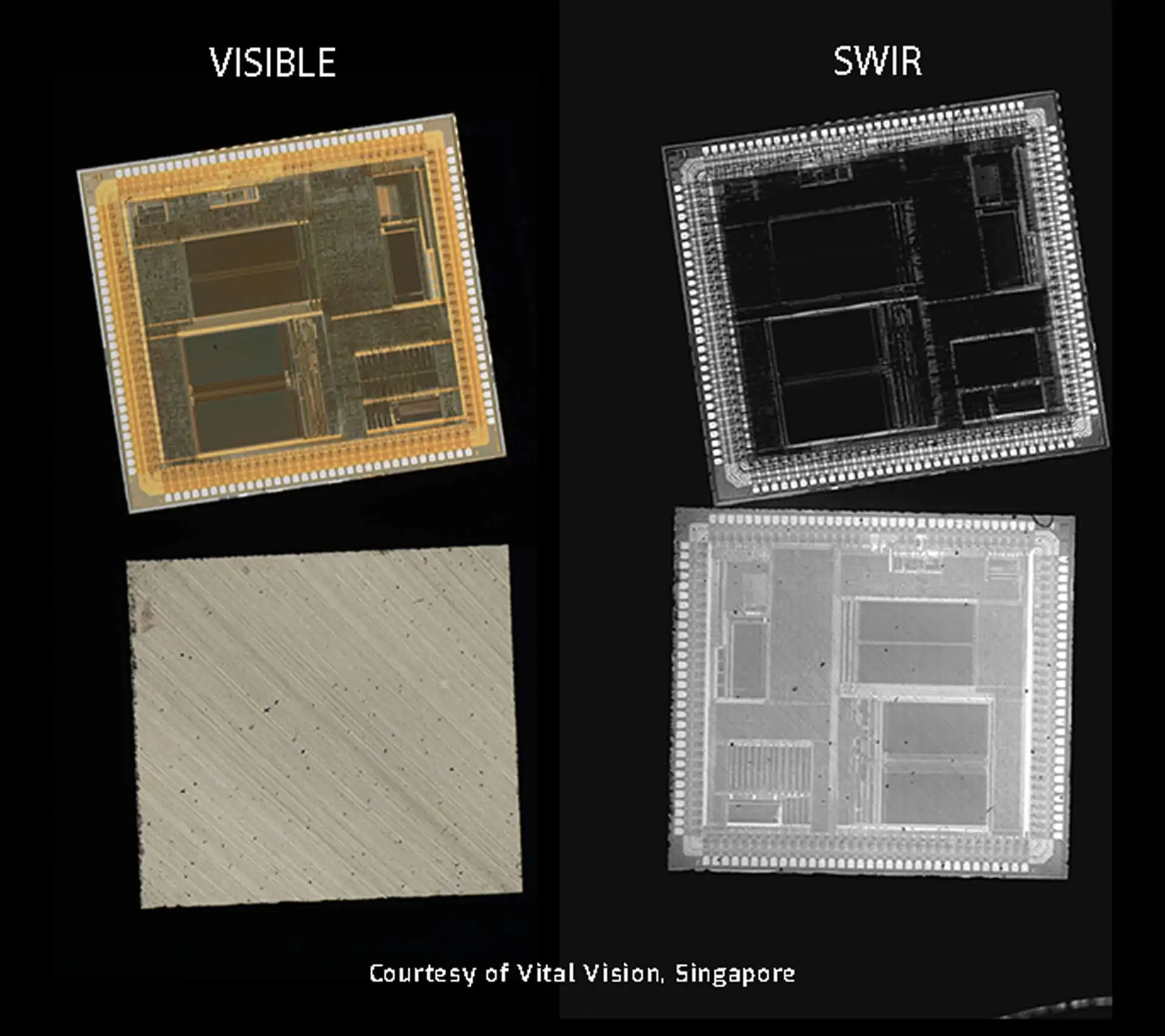
SWIR (Short-Wave Infrared) imaging enables visualization through silicon wafers, revealing internal structures, contamination, alignment issues, and hidden defects critical to semiconductor production and failure analysis.
With high sensitivity, low noise, and high dynamic range imaging, SWIR cameras improve inspection reliability, yield optimization, and process control across semiconductor manufacturing workflows.

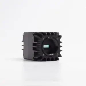
NIT SWIR Products
why NIT?
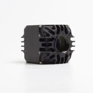
SWIR line-scan
Demonstration
Recommended products
Why NIT SWIR Cameras for Semiconductor Inspection?
SWIR band
High Resolution
(from line-scan 2K to Full HD resolution)
High Speed
(>110kHz with Line-scan camera )
Cost-effective solution
LiSaSWIR – The Ultimate Tool for Electronic Components, Silicon Wafers, and Solar Panels Inspection
Line-Scan SWIR Cameras
Line-scan SWIR cameras capture one line of pixels at a time as the object moves under the field of view. They are ideal for continuous or moving inspection processes such as:
- Wafer or substrate inspection on conveyor systems
- Web or roll-to-roll material analysis
- Inline defect detection during dicing or polishing
Advantages:
- Perfect for high-speed scanning and continuous processes
- Offers uniform illumination and consistent resolution across long surfaces
- Easily integrated into industrial automation systems
Demonstration images & videos
Recomended products
Industrial line-scan
High Sensitivity
High Sensitivity
Why Semiconductor Inspection Is Challenging
Modern semiconductor manufacturing involves increasingly complex inspection requirements:
- Defects are becoming smaller and more difficult to detect
- Many critical structures are hidden beneath silicon surfaces
- Conventional visible cameras cannot image through silicon
- Low contrast and high-speed production environments reduce inspection reliability
Missing defects can lead to:
- Yield loss
- Device reliability issues
- Increased production costs
- Delays in quality control and failure analysis
As semiconductor devices continue to shrink, imaging systems must provide higher sensitivity, improved contrast, and non-destructive inspection capability.
Why SWIR Imaging Improves Semiconductor Inspection
SWIR imaging operates in wavelength ranges where silicon becomes transparent, enabling inspection beyond the capabilities of visible imaging systems.
Unlike conventional visible cameras, SWIR cameras can visualize:
- Internal silicon structures
- Hidden defects
- Bonding alignment
- Through-silicon features
This makes SWIR imaging particularly valuable for:
- Wafer inspection
- Failure analysis
- Packaging inspection
- Semiconductor metrology
- Photovoltaic and solar cell inspection
- R&D and industrial process monitoring
Because SWIR captures reflected light rather than heat signatures, it provides detailed structural information with excellent image clarity.
Key Semiconductor Inspection Applications
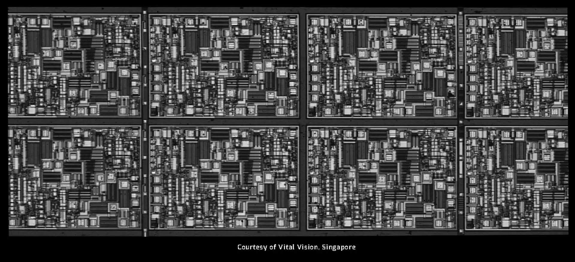
Wafer Inspection
SWIR imaging enables reliable wafer inspection by revealing:
- Cracks and fractures
- Surface contamination
- Structural defects
- Process irregularities
The ability to image through silicon improves inspection accuracy while reducing the need for destructive analysis methods.
Failure Analysis
SWIR cameras help engineers identify:
- Internal defects
- Bonding issues
- Packaging misalignment
- Defective interconnects
Subsurface imaging capability allows non-destructive investigation of integrated circuits and semiconductor packages.
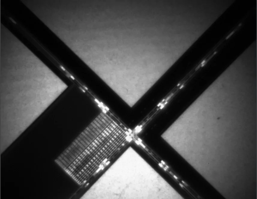
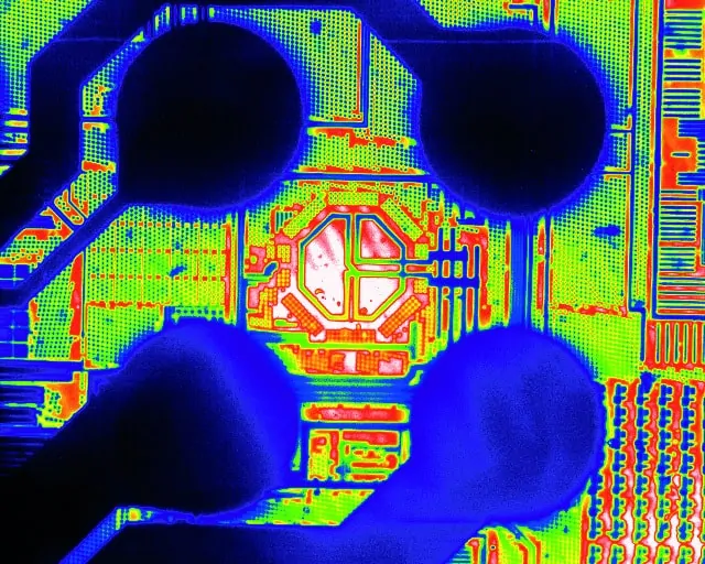
Semiconductor Packaging Inspection
Advanced packaging technologies require precise alignment and defect detection
SWIR imaging improves:
- Die alignment verification
- Bonding inspection
- Through-package imaging
- Multi-layer structure visualization
This is increasingly important for:
- 3D packaging
- wafer-level packaging
- heterogeneous integration
Solar Cell & Photovoltaic Inspection
SWIR imaging is widely used for:
- Microcrack detection
- Electroluminescence inspection
- Material uniformity analysis
- Process quality control
SWIR cameras enhance the visibility of defects that are invisible in standard visible imaging systems, thereby helping to increase manufacturing yield and reliability.
Why Camera Performance Matters
Semiconductor inspection systems require cameras capable of delivering:
- High sensitivity
- Low noise
- High resolution
- High dynamic range (HDR)
High-performance SWIR cameras enable:
- Detection of smaller defects
- Improved contrast in low-light conditions
- More reliable process monitoring
- Faster inspection workflows
This allows accurate inspection in complex semiconductor environments while maintaining excellent image quality.
SWIR Imaging Advantages for Semiconductor Applications
Silicon Transparency
Silicon becomes transparent in the SWIR spectrum, enabling subsurface imaging impossible with visible cameras.
Non-Destructive Inspection
SWIR imaging allows internal inspection without physically damaging components or wafers.
Improved Defect Detection
Enhanced contrast and sensitivity help reveal:
- Hidden cracks
- Delamination
- Contamination
- Alignment defects
Choosing the Right Imaging Technology
| Inspection Need | Recommended Technology |
|---|---|
| Through-silicon imaging | SWIR |
| Subsurface defect detection | SWIR |
| Thermal hotspot analysis | MWIR/LWIR |
| Standard surface inspection | Visible CMOS |
| High-contrast process inspection | SWIR + HDR |
Selecting the right wavelength range is essential for maximizing inspection performance and avoiding missed defects.
Frequently Asked Questions
Is SWIR imaging used in solar cell inspection?
Yes. SWIR cameras are widely used for photovoltaic inspection, including microcrack detection and material analysis.
Can SWIR cameras see through silicon?
Yes. Silicon becomes transparent in SWIR wavelengths, allowing imaging through wafers and semiconductor structures.
What is SWIR imaging used for in semiconductor inspection?
SWIR imaging is used to inspect silicon wafers, detect hidden defects, analyze semiconductor packages, and improve non-destructive failure analysis.
Why is SWIR better than visible imaging for wafer inspection?
Visible cameras cannot image through silicon. SWIR imaging enables subsurface inspection and improved defect detection.
What defects can SWIR detect?
SWIR cameras can detect:
- Cracks
- Contamination
- Bonding defects
- Internal structures
- Packaging misalignment
Improve Semiconductor Inspection with SWIR Imaging
SWIR imaging provides powerful capabilities for semiconductor manufacturing, inspection, and process optimization.
Whether you are developing advanced inspection systems, improving production yield, or performing semiconductor failure analysis, NIT SWIR cameras deliver the sensitivity and performance required for demanding industrial applications.
Request sample SWIR images
Discuss your semiconductor inspection application
