The semiconductor industry supports a vast amount of applications worldwide. Therefore, it should be no surprise that semiconductor inspection is highly important and must be optimized to ensure the quality and reliability of integrated circuits used in various electronic devices. Although there are several methods available for semiconductor inspection, SWIR (Short-Wave Infrared) imaging devices have emerged as powerful tools for this application. In this blog post, we will explore the applications, benefits, and key features of SWIR imaging devices in semiconductor inspection.
Understanding SWIR Imaging Devices
SWIR imaging provides enhanced sensitivity and image quality, enabling the detection of subtle defects that might go unnoticed with other technologies. Additionally, SWIR cameras offer non-destructive testing capabilities, allowing for thorough inspection without causing any damage to the semiconductor materials. Real-time monitoring and inspection automation are facilitated by SWIR cameras, improving efficiency and reducing the need for manual intervention. Furthermore, SWIR imaging devices are known for their cost-effectiveness, making them an attractive option for semiconductor manufacturers.
Learn more about how SWIR cameras work.
Applications of SWIR Imaging in Semiconductor Inspection
In the semiconductor industry, SWIR cameras are typically used to inspect ingots (silicon columns), thin wafers, and other semiconductor components, and they are also used for specific processing steps and failure analysis. Below, we look at these applications in more detail.
Bonding and Wire Detection
SWIR cameras can be used to inspect bonding and wire connections within integrated circuits. When these components are visualized, they enable users to identify problems such as detachment or misalignment and damaged wires.
Defect Detection and Classification
SWIR cameras are an outstanding choice of equipment for detecting and classifying defects such as cracks, particles, and micro-cracks in semiconductor components. They can penetrate silicon and other semiconductor materials, allowing for comprehensive inspection.
Wafer Inspection and Metrology
SWIR imaging devices enable accurate inspection and metrology of semiconductor wafers. They can be used to evaluate wafer alignment marks, critical dimensions, and overlay measurements, contributing to quality control in the manufacturing process.
Yield Improvement and Process Optimization
SWIR imaging devices are vital in improving yield and optimizing semiconductor manufacturing processes. They aid in identifying and rectifying process-related issues, reducing waste, and enhancing overall productivity.
SWIR imaging devices are regarded as invaluable tools in semiconductor inspection. Their ability to see through silicon and other semiconductor materials and enhanced sensitivity enable comprehensive defect detection and quality control. By utilizing SWIR imaging devices, semiconductor manufacturers can improve yields, optimize processes, and enhance overall productivity. Further innovations will likely enhance SWIR imaging for semiconductor inspection as technology advances.
New Imaging Technologies Offer SWIR Imaging Devices
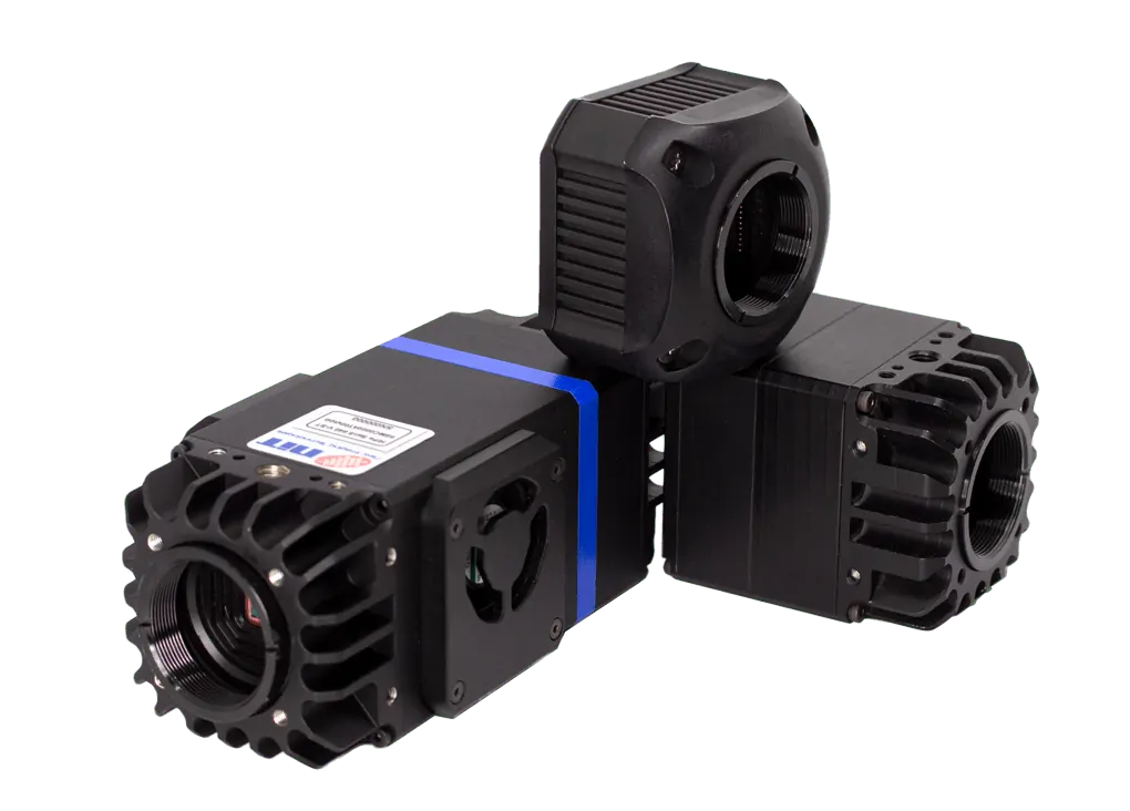
New Imaging Technologies (NIT) has established itself as a leading provider of SWIR sensors and cameras, offering a range of solutions for semiconductor inspection. Notably, NIT’s SWIR imaging devices offer a compelling performance-to-price ratio, making them highly suitable for integration into semiconductor production lines. With our advanced InGaAs material, proprietary manufacturing platforms, and expertise in ROIC, camera engineering, and CMOS design, NIT continues to provide SWIR solutions that combine exceptional performance and cost-effectiveness.
As the semiconductor industry evolves, NIT remains at the forefront of SWIR imaging technology, poised to contribute to further advancements in semiconductor inspection and quality control. With their commitment to innovation and customer satisfaction, NIT’s SWIR imaging devices are set to play an essential role in ensuring the reliability and efficiency of semiconductor manufacturing processes.
SWIR imaging solutions
To learn more about the SWIR imaging products we offer, contact a member of New Imaging Technologies today.


