Novel Stacking Technology for InGaAs to ROIC Bonding

Feb 9, 2021 | News

NIT is pleased to announce the release of several new SWIR sensors now produced with NIT in-house designed stacking technology, internally named NH.

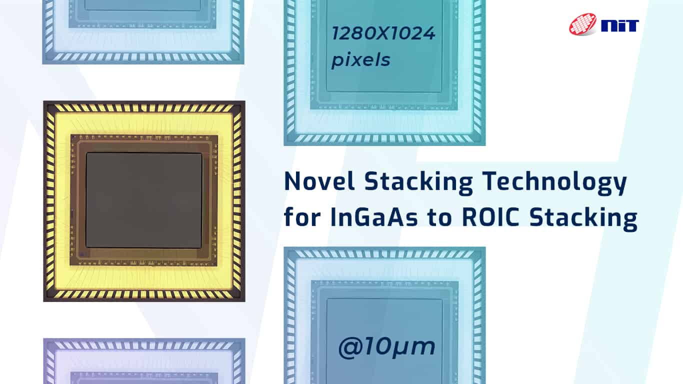
The NH technology allows to stack a photodiode array (PDA) of InGaAs to a CMOS read out circuit (ROIC) at pixel level. The NH technology does not rely on the classical Indium bump hybridization technique, therefore improving the manufacturing yield and lowering the sensor cost.

The VGA line of SWIR products with 15µm pitch is already in full production since several years using the NH technology.  New products with higher resolution and lower pitch from 10µm down to 7.5µm are currently under qualification, such as an HD array (1280×1024 pixels @ 10µm)

The roadmap towards very small pitch <5µm and Full HD+ formats is under construction at NIT.

Recent news

Using SWIR Imaging Devices in Semiconductor Inspection

Using SWIR Imaging Devices in Semiconductor Inspection

The semiconductor industry supports a vast amount of applications worldwide. Therefore, it should be no surprise that semiconductor inspection is highly important and must be optimized to ensure the quality and reliability of integrated circuits used in various...

What’s Next for Laser Communications Within SWIR Waveband?

What’s Next for Laser Communications Within SWIR Waveband?

The ever-growing demand for higher data rates, more cost-effective systems, higher bandwidths, and data security drives continuous innovation in laser communication. Free-space optical (FSO) communication systems are being continuously refined to meet these demands,...

How Does Laser Alignment Work?

How Does Laser Alignment Work?

Laser alignment is a vital process in many industrial and scientific applications as it ensures two or more components of a machine are aligned accurately. There are several internal and external techniques involved in laser alignment, including alignment for belts,...