Semiconductor inspection is a critical process in the electronics industry, ensuring the quality and reliability of integrated circuits. In recent years, Short-Wave Infrared (SWIR) imaging has emerged as a promising technology for semiconductor inspection due to its ability to penetrate silicon and other materials, offering valuable insights into the production process. However, SWIR imaging isn’t without its challenges. In this article, we’ll explore the obstacles posed by noise, calibration, and cost in SWIR semiconductor inspection, along with the solutions and advancements that are shaping the field.
Understanding SWIR Semiconductor Inspection
What is SWIR technology?
SWIR technology falls in the wavelength range of approximately 900 to 1700 nanometers. It allows for the detection and visualization of details that are otherwise invisible to the naked eye or traditional inspection techniques, making it a valuable tool in semiconductor inspection.
Role of SWIR Inspection in Semiconductor Manufacturing
Defect detection and identification are critical in semiconductor manufacturing to ensure the production of reliable and high-performance components. SWIR inspection plays a crucial role in this process by enabling the identification of defects that may otherwise go unnoticed. By providing detailed imaging and analysis, SWIR technology contributes to quality control and enhances efficiency in semiconductor production.
Challenges in SWIR Semiconductor Inspection
-
Noise:
Noise in SWIR images can degrade image quality, making defect detection and analysis difficult. This is particularly problematic in low-light conditions
-
Calibration:
Accurate calibration is crucial for precise semiconductor inspection. SWIR cameras must be calibrated to ensure consistent and reliable measurements, which can be complex and time-consuming.
-
Cost:
Historically, SWIR cameras have been expensive, limiting their widespread adoption for semiconductor inspection applications.
Solutions and Advancements
-
Noise Reduction Techniques:
Cutting-edge noise reduction algorithms are being developed to enhance SWIR image quality. These algorithms intelligently filter out noise while preserving essential details, improving defect detection accuracy.
-
Advanced Calibration Methods:
Researchers are working on automated calibration methods that reduce the need for manual adjustments. These advancements streamline the calibration process, minimizing downtime and increasing efficiency.
-
Cost-Effective SWIR Cameras:
Thanks to technological progress, the cost of SWIR cameras is gradually decreasing. This cost reduction opens opportunities for wider integration of SWIR imaging in semiconductor inspection processes.
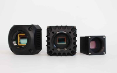
Semiconductor inspection with NIT SWIR cameras
For businesses looking to harness the benefits of SWIR semiconductor inspection, it’s essential to consider reliable and high-quality SWIR cameras.
New Imaging Technologies offers a range of SWIR cameras that are engineered to address the challenges mentioned above. These cameras boast cutting-edge noise reduction capabilities, advanced calibration mechanisms, and a cost-effective approach, making them an ideal choice for semiconductor inspection tasks.
SWIR semiconductor inspection holds significant promise for the electronics industry. While challenges like noise, calibration, and cost have posed obstacles, innovative solutions, and technological advancements are propelling the field forward. As the capabilities of SWIR cameras continue to evolve, businesses can confidently embrace this technology for more accurate and efficient semiconductor inspection processes.
SWIR imaging solutions
Contact NIT today for more information about our SWIR imaging solutions for semiconductor, silicon wafer & solar panel inspection.