SWIR Camera Backend Inspection: Seeing Through Silicon in Advanced Packaging
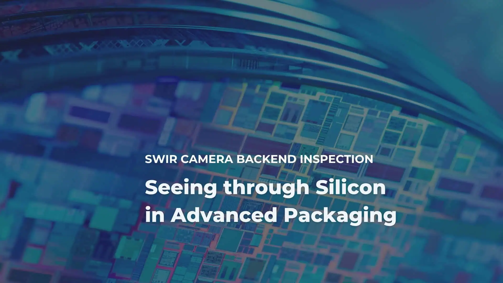
A SWIR camera backend inspection setup works because silicon is opaque in the visible range but transparent from ~900 to 1700 nm. An InGaAs SWIR camera therefore images through dies, wafers and interposers non-destructively, revealing the interfaces that determine packaging yield: die-attach voids, bond defects, bump/micro-bump misalignment, TSV fill quality and stacked-die alignment. The specs that decide feasibility are sensitivity and read-out noise (through-silicon imaging), dynamic range (bright metallization next to dark silicon).
The Imaging Problem in Backend
Most SWIR inspection content, including ours, concentrates on the front end: wafer surface, dicing, coating. The backend has a different inspection problem. Once a die is attached, interconnected and encapsulated, the critical interfaces, die-attach layer, interconnects, bump arrays, TSVs, are hidden under opaque silicon or inside the package. Destructive methods (cross-sectioning) and slow methods (acoustic microscopy, X-ray CT) don’t fit inline process control.
The relevant optical property: silicon, opaque in the visible range, becomes transparent across the SWIR band (~900–1700 nm and above). A properly specified InGaAs camera images through silicon layers, for alignement purpose, or revealing internal structures, contamination, cracks, or hidden defects like critical to semiconductor production and failure analysis. This article maps the backend inspection tasks where this capability applies, and – since NIT supplies the imaging component, not the inspection recipe, the camera specifications that determine whether the measurement is feasible.
Two points worth making explicitly:
- Through-silicon imaging requires sensitivity. Absorption through several hundred micrometers of silicon, plus interface losses, leaves a low light budget at the sensor. Camera sensitivity sets the detection floor – this is where sensor-level performance, not camera marketing, decides feasibility.
- Backend scenes mix extremes of reflectance. Metallization layers and wire bonds are specular and bright; silicon and mold compound are dark. A camera that clips the highlights to see the dark regions (or vice versa) corrupts both classes of measurement. True HDR capability – addresses this in a single exposure path.
SWIR Camera Backend Inspection, Camera Specification Checklist for Backend
- Sensitivity: measured QE across 900–1700 nm; read out noise in the operating temperature condition. Get the numbers.
- Dynamic range and its mechanism: single-exposure DR vs multi-response (dual-gain) HDR. Both have uses; know which the camera uses.
- Resolution and FOV: Full HD and HD sensors allow package-scale fields at bump-scale detail; line-scan for inline strip and panel inspection.
- Synchronization and interface: for inline integration with handlers and metrology automation.
SWIR Camera Backend Inspection:
Which NIT SWIR Sensors and Cameras fit Backend inspection?
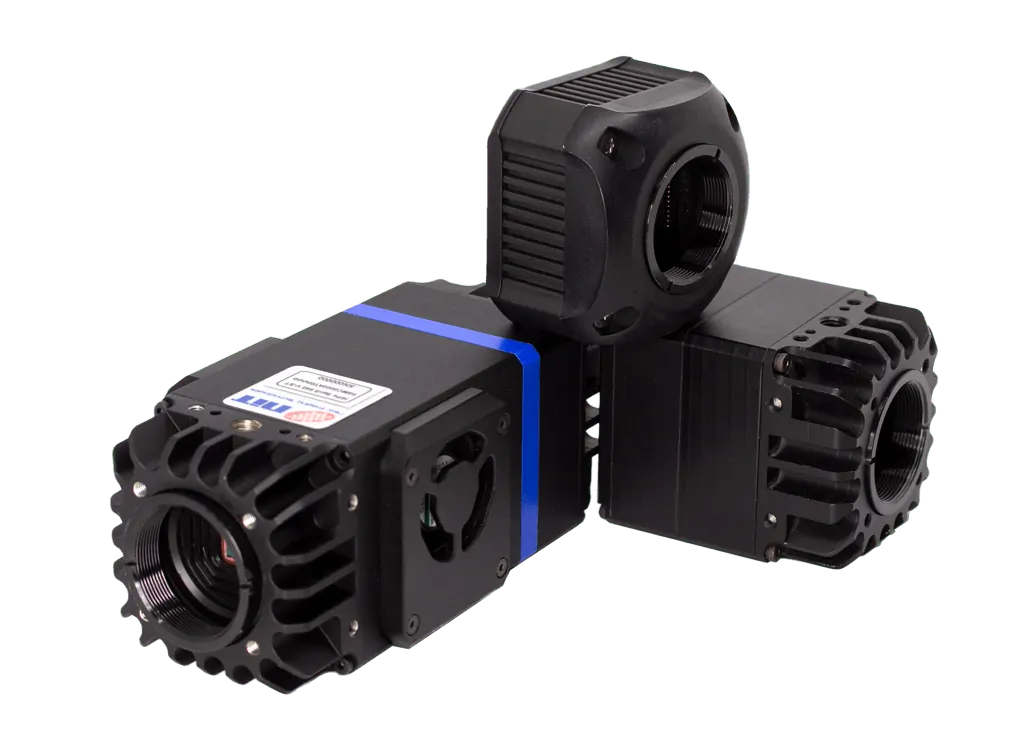
NIT, part of LYNRED, designs and manufactures its own SWIR InGaAs sensors and cameras in France – sensor fab to camera, one supply chain, Made in France, with engineering support available at the photodiode level for OEMs building inspection equipment.
Portfolio: line-scan (2048 px), qVGA, VGA, HD, Full HD, with performance options of high speed, high sensitivity / low noise, and high dynamic range.
Typical fits for backend imaging tasks:
-
SenS 1280
HD, high sensitivity. The photon-starved through-silicon configurations (die-attach voids, bond inspection) are where low-noise high-sensitivity sensors earn their selection.
-
SenS 1920
Full HD, high sensitivity. Package-scale and wafer-scale fields at bump-level detail.
-
WiDy SenS 320 / WiDy SenS 640
High-speed, dual-response HDR area cameras for scenes combining metallization and silicon; useful when one exposure must serve both bright and dark regions.
-
LiSaSWIR 2048 v2
2K line-scan for inline strip, substrate and panel-level packaging inspection.
SWIR Camera Backend Inspection – FAQ
Why use a SWIR camera for backend inspection instead of a visible camera?
Silicon is opaque in the visible range, so visible cameras only see the package surface. A SWIR InGaAs camera images through silicon layers (~900–1700 nm and above) — for alignment purposes, or to reveal internal structures, contamination, cracks and hidden defects critical to semiconductor production and failure analysis.
Can a SWIR camera replace cross-sectioning or acoustic microscopy?
Not entirely. Destructive and slow methods don’t fit inline process control, and SWIR camera backend inspection doesn’t cover every defect type. SWIR provides fast, non-destructive, inline-capable through-silicon imaging.
SWIR camera backend inspection
Through-Silicon SWIR Imaging for Backend and Advanced Packaging Inspection
Feasibility of a given through-silicon measurement depends on your stack (thickness, doping, backside treatment) and illumination.
Contact NIT today for more information about our SWIR imaging solutions for this application.