Join us at SPIE Baltimore 2019, discover Additive Manufacturing part 2

Mar 19, 2019 | News

NIT will present at booth#224 at SPIE Defense & Commercial Sensing, Baltimore, USA from April 16th to 18th, 2019. Find out what NIT bring to SPIE. Until then, discover how SWIR cameras work in the laser process, in this case, additive manufacturing.

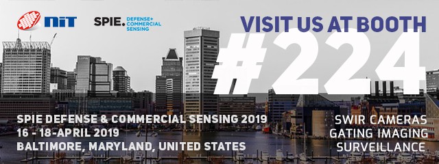
Join us at SPIE Baltimore.
Attending SPIE Defense & Commercial sensing 2019? We’re excited to meet you at booth #224 and share our expert guidance, technologies, and SWIR products for advancing your vision ability in your application.

What we bring to SPIE 2019

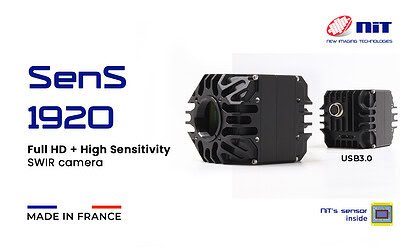
This year, at SPIE 2019, we will introduce our high-end camera WiDy SenS with new advanced updates. This new version of WiDy SenS makes it a cost-effective solution for your imaging challenge.

Our WiDy SenS series, High Sensitivity & High Dynamic Range SWIR cameras, with the Gated mode option, are capable of providing high-quality images in all lighting conditions.

Don’t miss the chance to test our SWIR cameras’ performances on-site and discuss with our experts to get the cutting-edge SWIR products.
Schedule our meeting in advance to have a quality discussion.

See you there from April 16th -18th, 2019!

Get to know more our SWIR cameras in action.

With many advantages of NIT SWIR cameras, such as HDR patented technology, anti-blooming native functions, high frame rate, working with lasers become simpler.

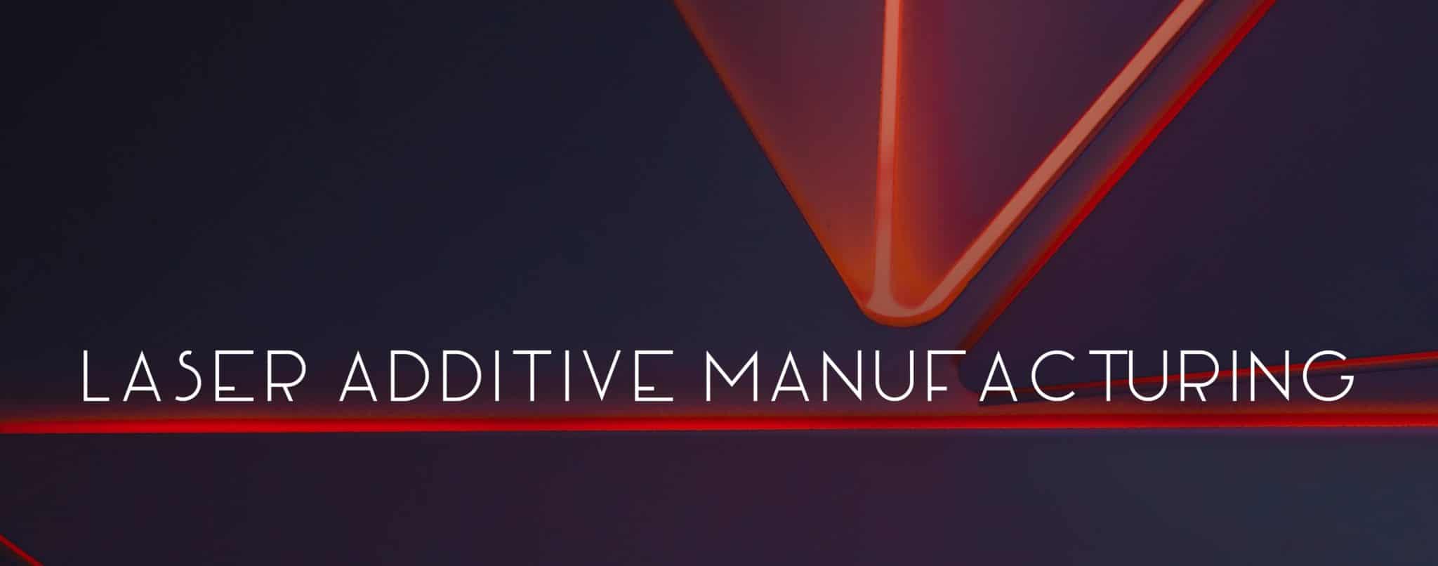
Following the first part of our case study – Additive manufacturing, this time, discover how our SWIR cameras give the ability to bring an extra eye on the melt pool or any similar conditions.

Want to get notification of our news?

Recent news

Introducing SenS 1280: HD SWIR Camera – Smart Version

Introducing SenS 1280: HD SWIR Camera – Smart Version

SenS 1280 - Smart version Introducing the SenS 1280 HD SWIR camera - Smart version, developed and produced in France. This camera delivers crisp, low-noise images with its impressive features: HD resolution, automatic gain control, and advanced image processing...

Using SWIR Imaging Devices in Semiconductor Inspection

Using SWIR Imaging Devices in Semiconductor Inspection

The semiconductor industry supports a vast amount of applications worldwide. Therefore, it should be no surprise that semiconductor inspection is highly important and must be optimized to ensure the quality and reliability of integrated circuits used in various...

What’s Next for Laser Communications Within SWIR Waveband?

What’s Next for Laser Communications Within SWIR Waveband?

The ever-growing demand for higher data rates, more cost-effective systems, higher bandwidths, and data security drives continuous innovation in laser communication. Free-space optical (FSO) communication systems are being continuously refined to meet these demands,...