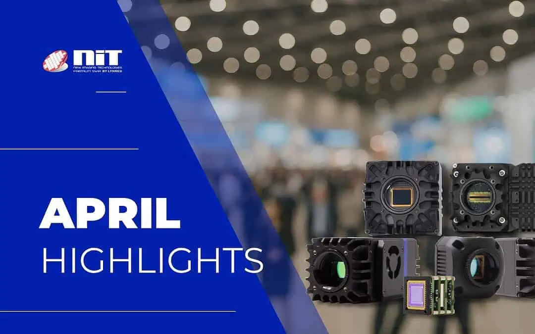
New Imaging Technologies (NIT) continues to expand its SWIR offering this April, combining product innovation with enhanced tools for system integration.
Throughout the month, NIT will engage with industry professionals at key international events while showcasing its latest high-performance SWIR sensors and cameras, including solutions with up to Full HD resolution and advanced line-scan capabilities. These SWIR solutions are designed to meet the growing demands of industrial, scientific, and defense applications.
Line-scan SWIR cameras for high-speed inspection (including NEW rectangular-pixel variant for improved measurement precision)
April’s event highlights:
Throughout the month, our team will be actively engaging with industry professionals across key international gatherings:
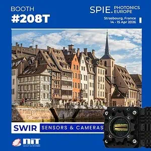
SPIE Photonics Europe – Strasbourg, France (14–15 April 2026)
In Europe, our sales leadership team—including our Director of Sales, Régis Tulaza, and Sales Area Manager, Martin du Tertre will be available at Booth 208 to discuss how our SWIR solutions can address your specific needs.
SPIE Defense + Security | National Harbor, MD, USA | 28–30 April 2026
In the United States, our General Manager, François Coursaget, will represent our SWIR activities within the LYNRED team at the LYNRED USA booth. A dedicated presentation on recent advances in SWIR sensor technology will also be delivered, offering insights into our ongoing innovation efforts.
Whether you are exploring new imaging capabilities or optimizing existing systems, our team remains committed to supporting your projects with cutting-edge SWIR technology.
If you would like to schedule a dedicated discussion or learn more about our solutions, feel free to get in touch.
NIT’s camera CAD models now available
NIT is pleased to introduce a new resource designed to support engineers and integrators
3D STEP files for NIT’s SWIR cameras are now accessible via the Download page, enabling faster and more efficient system development.
The files cover a range of NIT’s camera platforms, including high-performance and line-scan SWIR solutions and CMOS models.
As solar farms scale worldwide, operators are seeking faster, more reliable inspection methods to maximize energy output and reduce maintenance costs. Traditional inspection methods, based on visible or thermal imaging, often fail to detect early-stage defects. Short-Wave Infrared (SWIR) imaging integrated on drones is emerging as a powerful solution for advanced solar panel inspection, enabling the detection of defects invisible to conventional visible or thermal imaging.
Why Traditional Inspection Methods Fall Short
Conventional inspection technologies have clear limitations. Visible imaging depends heavily on lighting conditions and cannot reveal subsurface defects. Thermal imaging, while useful for identifying hotspots, typically detects issues only after they have already affected performance.
As a result, many critical defects—such as micro-cracks, early delamination, or moisture ingress—remain undetected during routine inspections. This can lead to reduced energy output, unexpected failures, and increased maintenance costs.
High-Performance InGaAs SWIR Solutions for Aerial PV Monitoring
New Imaging Technologies (NIT), part of LYNRED, a leading designer and manufacturer of high-performance SWIR InGaAs sensors and cameras, supports this application with a complete range of lightweight, high-resolution SWIR imaging solutions optimized for UAV integration.
Why SWIR Drone-Based Inspection for Solar Panel Farm?
SWIR Drone-Based Inspection: Enabling the Next Generation of Solar Farm Monitoring
The integration of SWIR imaging into drone inspection workflows opens the door to data-driven solar asset management. High-quality SWIR data can be combined with analytics and AI tools to automate defect detection, prioritize maintenance, and optimize system performance.
As solar farms continue to grow in scale and complexity, the need for accurate, efficient, and scalable inspection technologies will only increase. SWIR drone imaging stands out as a future-proof solution that delivers both precision and operational efficiency.
By combining SWIR imaging and drone technology, solar operators gain access to more precise diagnostics, earlier fault detection, and higher inspection efficiency.
With its complete portfolio of SWIR sensors, modules, and cameras, NIT supports UAV manufacturers, system integrators, and solar inspection specialists in deploying reliable, high-performance aerial inspection solutions.
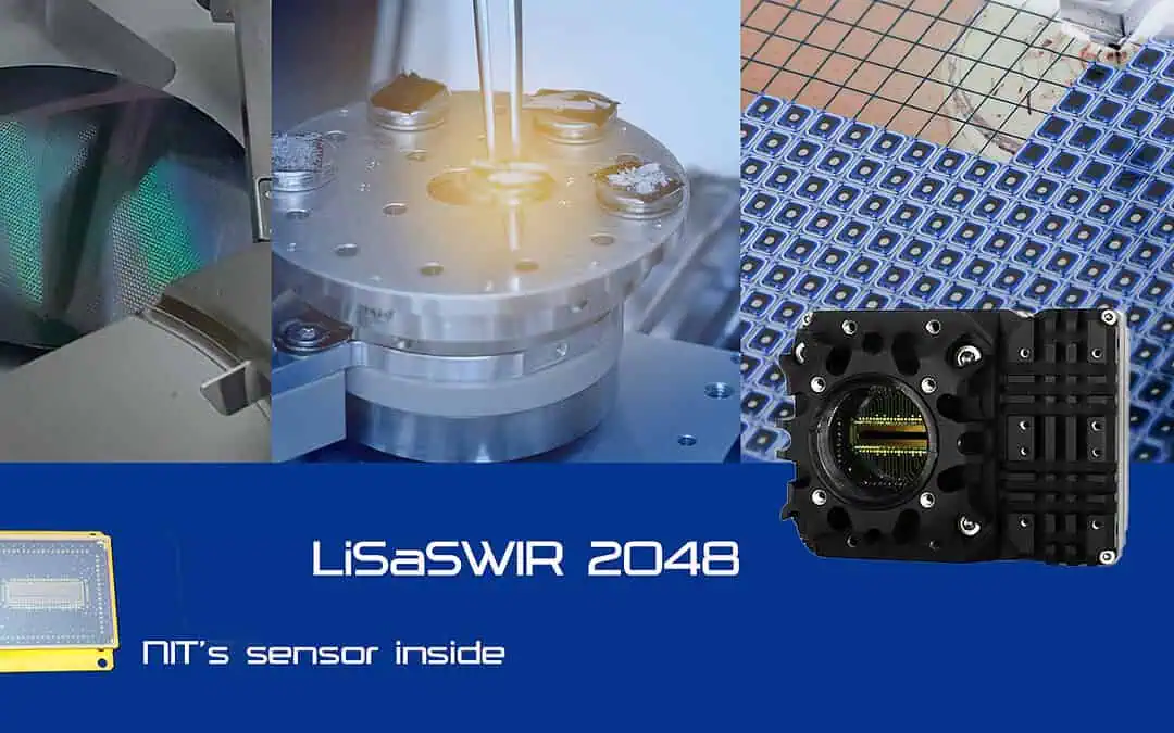
New Imaging Technologies (NIT), a LYNRED company, announces that theLiSa SWIR 2048R M-STE2 is now available for order. The camera was first presented at SPIE Photonics West 2026 and is now ready for commercial deployment.
Rectangular-Pixel SWIR Camera
The LiSa SWIR 2048R is a rectangular-pixel SWIR camera optimized for Spectroscopy and Optical Coherence Tomography (OCT). Based on the provenLiSa SWIR 2048 v2 platform, it features a rectangular pixel format (8 × 200 µm) designed for spectroscopic and line-scan optical architectures, enabling efficient light collection and high signal performance in demanding applications.
The LiSa SWIR camera family also includes the LiSa SWIR 2048 standard version, a line-scan SWIR camera widely used in industrial inspection applications such as material sorting, semiconductor inspection, and quality control, where reliability, sensitivity, and robustness are critical.
With the commercial availability of theLiSa SWIR 2048R, NIT further expands its LiSa SWIR portfolio, offering tailored SWIR camera solutions forindustrial, scientific, and medical instrument manufacturers.
For ordering information or technical details, don’t hesitate to get in touch with NIT
Rectangular-Pixel SWIR Camera
Contact NIT today for more information about our LiSaSWIR2048R and its applications.
NIT Launches LiSa SWIR 2048R M-STE2, Rectangular SWIR Camera at SPIE Photonics West 2026
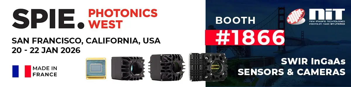
New Imaging Technologies (NIT) announces the launch of LiSa SWIR 2048R M-STE2, a new rectangular-pixel SWIR camera based on the proven LiSaSWIR 2048 v2 platform. The new camera will be officially introduced at SPIE Photonics West 2026, taking place from January 20 to 22, 2026, in San Francisco, USA.
The LiSa SWIR 2048R M-STE2 has been specifically designed for hyperspectral imaging, spectroscopy, and Optical Coherence Tomography (OCT) applications. It features a rectangular pixel format of 8 × 200 µm, optimized for line-scan and spectroscopic optical architectures. This geometry enables efficient light collection and enhanced performance in applications requiring precise spectral information.
Rectangular pixel (8×200µm)
Application: Hyperspectral imaging, spectroscopy, OCT
By extending the LiSa SWIR 2048 v2 camera into a rectangular format, NIT expands its LiSa SWIR camera family, offering system integrators and instrument manufacturers greater flexibility for advanced SWIR system designs while maintaining the performance, reliability, and robustness expected from NIT solutions.
Upcoming launch at SPIE Photonics West 2026
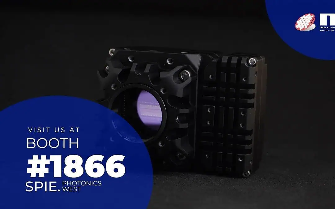
NIT will showcase the LiSa SWIR 2048R M-STE2 SWIR camera at booth #1866 during SPIE Photonics West 2026. Visitors are invited to meet the NIT team to learn more about this new camera and discuss application requirements.
Meet the NIT team on site:
Régis Tulaza – Director of Sales
Martin du Tertre – Regional Sales Manager
Martin Schweitzer -Technical Manager
About New Imaging Technologies (NIT)
New Imaging Technologies (NIT), a Lynred company, designs and manufactures high-performance SWIR cameras and image sensors for scientific, industrial, and defense applications.
Discover Rectangular SWIR camera at SPIE Photonics West
Be among the first to discover the LiSa SWIR 2048R
2025 SWIR Camera Performance Milestones and Prepares for 2026
As 2025 comes to a close, New Imaging Technologies (NIT) highlights the key achievements that have shaped its SWIR camera roadmap over the past year. Throughout 2025, NIT continued to strengthen its position as a leading designer and manufacturer of Short-Wave Infrared (SWIR) cameras, focusing on performance, system integration, and reliability for industrial inspection, scientific, and defense applications.
Driven by growing market demand for higher speed, higher resolution, and easier integration, NIT’s developments in 2025 addressed the evolving requirements of advanced imaging systems.
High-Speed and High-Resolution Line-Scan SWIR Camera Performance
One of the most significant milestones of 2025 was the advancement of line-scan SWIR camera technology, achieving line rates above 110 kHz for high-throughput applications. These speeds enable faster inspection processes in environments where productivity and accuracy are critical.
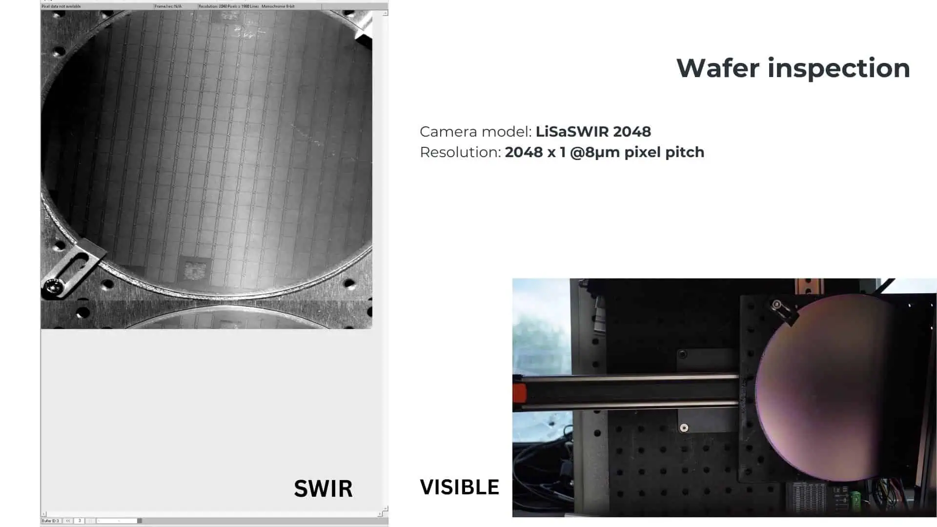
In parallel, NIT introduced a new line-scan generation, LiSaSWIR 2048 v2, featuring a 2048 × 1 resolution with an 8 µm pixel pitch, combining increased spatial resolution with high acquisition speed. This evolution supports more detailed inspection while maintaining the throughput required in industrial inspection and related applications.
These capabilities are exemplified by the latest line-scan developments, which are designed to support demanding use cases such as materials inspection, semiconductor processing, and Optical Coherence Tomography (OCT), where both speed and precision are essential.
High-Speed Area-Scan SWIR Imaging for Dynamic Applications
In the area-scan segment, NIT continued to push the limits of high-speed SWIR imaging. During 2025, its SWIR cameras enabled frame rates of up to 1 kHz full-frame, with up to 10 kHz in region-of-interest (ROI) modes.
These high frame rates, combined with ultra-short exposure times, enable the accurate capture of fast, dynamic scenes while maintaining image quality and sensitivity. Such performance is particularly relevant for applications involving motion analysis, real-time monitoring, and time-critical imaging processes.
By expanding both line-scan and area-scan performance, NIT reinforced its ability to address a wide range of SWIR imaging requirements using consistent technologies and platforms.
OEM-Optimized SWIR Camera Platforms and Interfaces
Beyond raw performance, 2025 also marked continued progress in OEM-optimized SWIR camera architecture. NIT focused on delivering compact, rugged, and integration-ready platforms designed to simplify system development for industrial and defense customers. These platforms support a variety of interfaces and system configurations, enabling reliable board-to-board and board-to-cable integration while maintaining robustness in challenging operational environments. This approach reflects NIT’s long-term commitment to supporting embedded system designers and system integrators with SWIR cameras that are both high-performance and practical to deploy.
During 2025, Full HD SWIR cameras, SenS 1920, achieved successful integration into advanced industrial and defense systems. These integration successes confirm the maturity and reliability of NIT’s high-resolution SWIR imaging solutions in demanding operational conditions.
By combining Full HD resolution with optimized interfaces and stable performance, NIT’s SWIR cameras continue to meet the expectations of customers developing complex imaging systems with long lifecycle requirements.
Looking Ahead to 2026: Meet NIT at SPIE Photonics West
SWIR cameras will be presented at NIT’s booth, SPIE Photonics West 2026
Looking forward, NIT will continue to advance its SWIR camera portfolio in 2026, with a focus on performance scalability, integration efficiency, and application-driven innovation.
NIT invites customers and partners to meet its team at SPIE Photonics West 2026, taking place in San Francisco, California, from January 20 to 22, 2026, at Booth #1866.
Visitors will have the opportunity to explore NIT’s comprehensive SWIR camera portfolio, spanning line-scan to Full HD, and discuss upcoming projects with NIT and LYNRED experts, who will also be present to share their expertise in infrared technologies.
Season’s Greetings and Office Closure
NIT thanks its customers, partners, and collaborators for their continued trust throughout 2025 and wishes everyone a Merry Christmas and a Happy New Year.
Please note that NIT offices will be closed on December 25, 2025, and January 1, 2026.
About New Imaging Technologies (NIT)
New Imaging Technologies (NIT) designs and manufactures high-performance SWIR sensors and SWIR cameras for industrial inspection, scientific research, defense, and medical applications. Based in France, NIT delivers advanced SWIR imaging solutions optimized for demanding environments and system-level integration.
High-speed SWIR cameras and line-scan SWIR cameras are becoming essential tools for modern industrial inspection, semiconductor manufacturing, laser monitoring, and other advanced imaging fields where speed, sensitivity, and reliability are critical. As demand for higher throughput and better detection capabilities grows, Short-Wave Infrared (SWIR) imaging provides unique advantages by revealing details invisible to standard visible cameras. In this article, we explore how SWIR imaging enhances high-speed industrial inspection workflows and how different SWIR camera architectures—line-scan and area-scan—fit into various application needs.
Challenges in Semiconductor Inspection
Semiconductor manufacturing demands exceptional precision and reliability at every stage — from wafer fabrication to packaging. Detecting micro-defects such as cracks, contamination, or pattern irregularities is crucial to maintain high yield and prevent costly failures.
Traditional visible-light cameras often fail to reveal such defects because silicon, the primary material in semiconductor devices, is opaque to visible light but transparent in the Short-Wave Infrared (SWIR) spectrum. As a result, a high-speed SWIR camera becomes a critical tool for detecting defects hidden beneath silicon surfaces.
As inspection lines move toward higher speeds and smaller geometries, manufacturers require high-performance SWIR cameras(Line-scan, Area-scan) that can deliver excellent image quality, speed, and stability under demanding industrial conditions.
Detecting Micro-Defects with High-Speed SWIR Cameras
SWIR cameras enable engineers to see beyond the visible spectrum, revealing information invisible to traditional imaging systems. In semiconductor production, they are used for:
Wafer and die inspection: Detecting micro-cracks, edge chips, and surface irregularities.
Bond and interconnect analysis: Inspecting layers and verifying bonding integrity.
Encapsulation and packaging inspection: Identifying trapped particles or voids in encapsulant materials.
NIT’s high-speed SWIR cameras are built around proprietary InGaAs sensor technology designed for high sensitivity, low noise, and high dynamic range. These features ensure reliable defect detection, even in high-reflectance environments typical of semiconductor manufacturing.
Line-Scan vs Area-Scan SWIR Cameras
Choosing between a line-scan and an area-scan SWIR camera depends on the inspection setup, the object’s motion, and the required resolution.
Line-Scan SWIR Cameras
Line-scan SWIR cameras capture one line of pixels at a time as the object moves under the field of view. They are ideal for continuous or moving inspection processes such as:
Wafer or substrate inspection on conveyor systems
Web or roll-to-roll material analysis
Inline defect detection during dicing or polishing
Advantages:
Perfect for high-speed scanning and continuous processes
Offers uniform illumination and consistent resolution across long surfaces
Easily integrated into industrial automation systems
Considerations:
Requires precise synchronization between the camera and object motion
Not suited for static or randomly positioned samples
LiSaSWIR 2048 v2 – New Line-scan SWIR camera Ideal for semiconductor inspection lines requiring high resolution, high speed, and excellent uniformity. Its 2048-pixel resolution delivers outstanding defect and edge detection on silicon wafers and semiconductor substrates.
LiSaSWIR 2048 image example
Area-Scan SWIR Cameras
Area-scan cameras capture a full image frame at once, making them suitable for stationary or small field-of-view inspection tasks. These cameras are particularly effective for detailed defect analysis, component inspection, or laboratory evaluation.
NIT offers a complete range of area-scan SWIR cameras, from QVGA to Full HD resolution, enabling users to choose the best fit for their inspection needs — from compact, high-speed sensors to large-format, high-resolution imaging systems.
Advantages:
Provides instant full-field images, ideal for stationary samples or slow-moving processes
Supports high-resolution imaging for fine defect analysis
More flexible setup — no motion control required
Considerations:
Limited by frame rate for continuous line inspections
May require higher bandwidth interfaces for large-format models
SenS 1920 — Full HD resolution, high sensitivity Perfect for applications requiring maximum detail, extremely low noise, and Full HD format for micro-defect characterization.
SenS 1280 — HD resolution, GenICam compliant An excellent choice for system integrators needing industrial standards, flexibility, and high sensor performance in a robust format.
Recommendation:
Choose line-scan SWIR cameras for continuous, high-speed wafer or substrate inspection.
Choose area-scan SWIR cameras for detailed defect review, lab analysis, or applications requiring high spatial resolution.
Boosting Yield and Quality Control
By integrating high-speed SWIR cameras into semiconductor inspection systems, manufacturers can detect hidden defects earlier in the process, reduce rework, and improve overall production yield.
NIT’s SWIR imaging solutions combine:
High resolution
High sensitivity for low-reflectivity surfaces
High dynamic range for mixed-brightness scenes
High frame rates for inline inspection
These features make NIT’s cameras a powerful tool for semiconductor manufacturers seeking to increase throughput while maintaining stringent quality standards.
Take the Next Step with NIT
As a SWIR camera designer and manufacturer based in France, New Imaging Technologies (NIT) offers a full range of SWIR imaging solutions — from line-scan cameras for high-speed inspection to Full HD area-scan systems for detailed analysis.
Get your best SWIR products
Whetheryouneed standard products or customized interfaces for integrationintoyour inspection line, NIT provides the flexibility and expertise to meetyourrequirements.