Watch our demo to see the advantages of NIT SWIR cameras for semiconductor inspection
SWIR for inspection – Reveal the heart of your material.
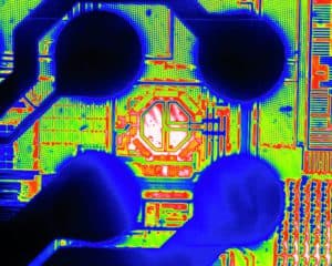
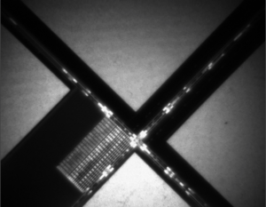
For the past years, the SWIR band has been recognized as one of the best wavelength regions for industrial inspection. Whether detecting cracks or defects on a wafer or solar cells panels, InGaAs imaging devices are suited for seeing through silicon.
With HDR patented technology, high sensitivity, and a plug-and-play integration, NIT SWIR cameras, especially WiDy SenS, can help inspection process easier, more accurate and cost-effective.
Our demonstration, featuring NIT WiDy SenS and Effilux SWIR backlight, illustrates the advantages of NIT SWIR cameras versus visible cameras in detecting defects, trapped air and component observation for a silicon wafer.
Thanks, Effilux for this collaboration.
Happy to help.
NIT experts team is always available for all your needs. Please feel free to contact us to get your answers as soon as possible.
About WiDy SenS
Among the WiDy family, the WiDy SenS offers the highest sensitivity in the SWIR band, makes it suitable for Semiconductor inspection. Thanks to a small pixel pitch of 15µm, the WiDy SenS camera can easily be used in a microscope inspection machine for small defect detections. The WiDy SenS cameras come with a 46x46x57mm3 form factor and represent a cost-effective solution for integration into a semiconductor production line.