Introduction
High-speed SWIR cameras and line-scan SWIR cameras are becoming essential tools for modern industrial inspection, semiconductor manufacturing, laser monitoring, and other advanced imaging fields where speed, sensitivity, and reliability are critical. As demand for higher throughput and better detection capabilities grows, Short-Wave Infrared (SWIR) imaging provides unique advantages by revealing details invisible to standard visible cameras. In this article, we explore how SWIR imaging enhances high-speed industrial inspection workflows and how different SWIR camera architectures—line-scan and area-scan—fit into various application needs.
Challenges in Semiconductor Inspection
Semiconductor manufacturing demands exceptional precision and reliability at every stage — from wafer fabrication to packaging. Detecting micro-defects such as cracks, contamination, or pattern irregularities is crucial to maintain high yield and prevent costly failures.
Traditional visible-light cameras often fail to reveal such defects because silicon, the primary material in semiconductor devices, is opaque to visible light but transparent in the Short-Wave Infrared (SWIR) spectrum. As a result, a high-speed SWIR camera becomes a critical tool for detecting defects hidden beneath silicon surfaces.
As inspection lines move toward higher speeds and smaller geometries, manufacturers require high-performance SWIR cameras (Line-scan, Area-scan) that can deliver excellent image quality, speed, and stability under demanding industrial conditions.
Detecting Micro-Defects with High-Speed SWIR Cameras
SWIR cameras enable engineers to see beyond the visible spectrum, revealing information invisible to traditional imaging systems. In semiconductor production, they are used for:
- Wafer and die inspection: Detecting micro-cracks, edge chips, and surface irregularities.
- Bond and interconnect analysis: Inspecting layers and verifying bonding integrity.
- Encapsulation and packaging inspection: Identifying trapped particles or voids in encapsulant materials.
NIT’s high-speed SWIR cameras are built around proprietary InGaAs sensor technology designed for high sensitivity, low noise, and high dynamic range. These features ensure reliable defect detection, even in high-reflectance environments typical of semiconductor manufacturing.
Line-Scan vs Area-Scan SWIR Cameras
Choosing between a line-scan and an area-scan SWIR camera depends on the inspection setup, the object’s motion, and the required resolution.
Line-Scan SWIR Cameras
Line-scan SWIR cameras capture one line of pixels at a time as the object moves under the field of view. They are ideal for continuous or moving inspection processes such as:
- Wafer or substrate inspection on conveyor systems
- Web or roll-to-roll material analysis
- Inline defect detection during dicing or polishing
Advantages:
- Perfect for high-speed scanning and continuous processes
- Offers uniform illumination and consistent resolution across long surfaces
- Easily integrated into industrial automation systems
Considerations:
- Requires precise synchronization between the camera and object motion
- Not suited for static or randomly positioned samples
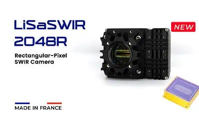
LiSaSWIR 2048 v2 – New Line-scan SWIR camera
Ideal for semiconductor inspection lines requiring high resolution, high speed, and excellent uniformity. Its 2048-pixel resolution delivers outstanding defect and edge detection on silicon wafers and semiconductor substrates.
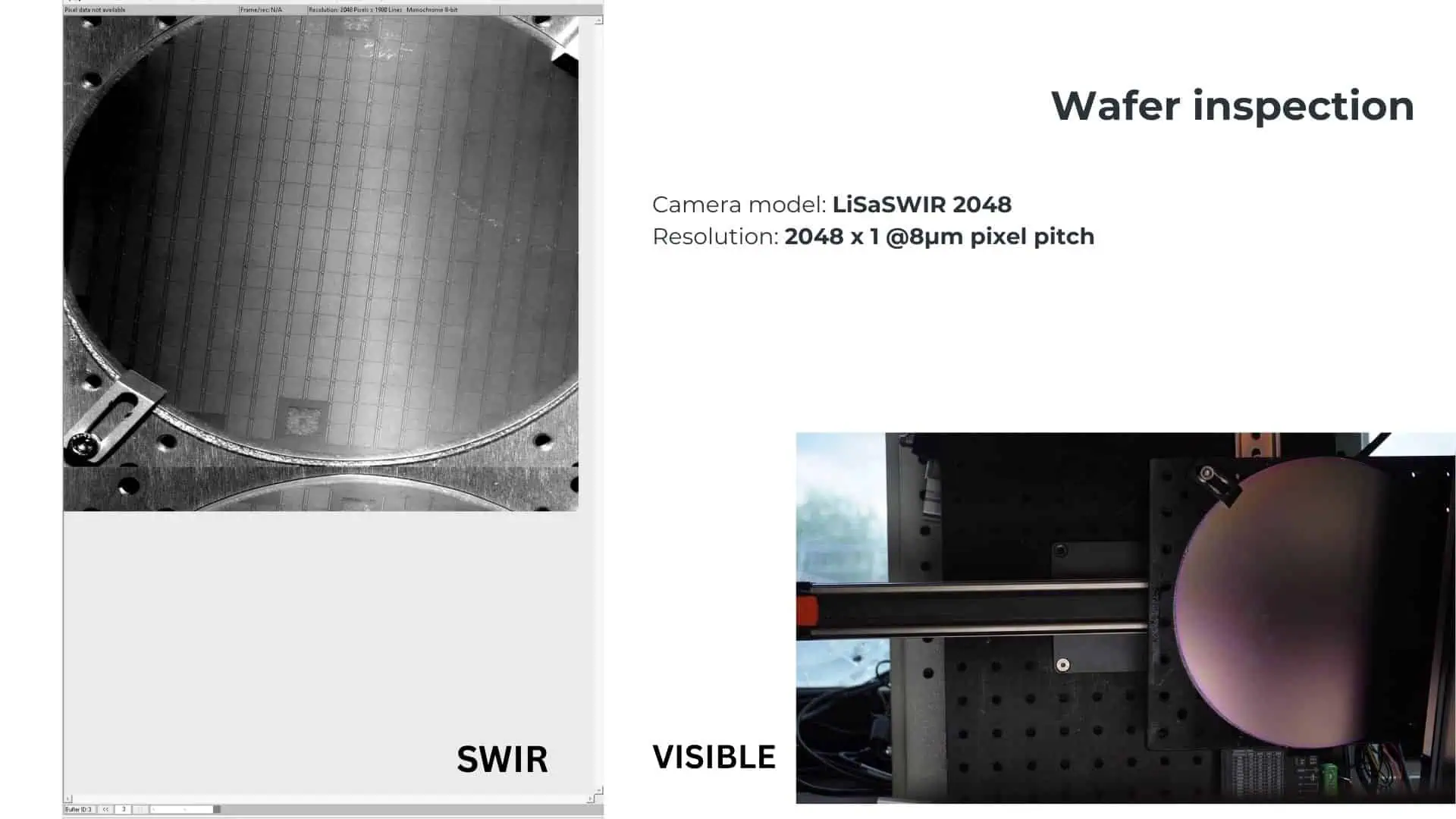
LiSaSWIR 2048 image example
Area-Scan SWIR Cameras
Area-scan cameras capture a full image frame at once, making them suitable for stationary or small field-of-view inspection tasks. These cameras are particularly effective for detailed defect analysis, component inspection, or laboratory evaluation.
NIT offers a complete range of area-scan SWIR cameras, from QVGA to Full HD resolution, enabling users to choose the best fit for their inspection needs — from compact, high-speed sensors to large-format, high-resolution imaging systems.
Advantages:
- Provides instant full-field images, ideal for stationary samples or slow-moving processes
- Supports high-resolution imaging for fine defect analysis
- More flexible setup — no motion control required
Considerations:
- Limited by frame rate for continuous line inspections
- May require higher bandwidth interfaces for large-format models
SenS 1920 — Full HD resolution, high sensitivity
Perfect for applications requiring maximum detail, extremely low noise, and Full HD format for micro-defect characterization.SenS 1280 — HD resolution, GenICam compliant
An excellent choice for system integrators needing industrial standards, flexibility, and high sensor performance in a robust format.
Recommendation:
- Choose line-scan SWIR cameras for continuous, high-speed wafer or substrate inspection.
- Choose area-scan SWIR cameras for detailed defect review, lab analysis, or applications requiring high spatial resolution.
Boosting Yield and Quality Control
By integrating high-speed SWIR cameras into semiconductor inspection systems, manufacturers can detect hidden defects earlier in the process, reduce rework, and improve overall production yield.
NIT’s SWIR imaging solutions combine:
- High resolution
- High sensitivity for low-reflectivity surfaces
- High dynamic range for mixed-brightness scenes
- High frame rates for inline inspection
These features make NIT’s cameras a powerful tool for semiconductor manufacturers seeking to increase throughput while maintaining stringent quality standards.
Take the Next Step with NIT
As a SWIR camera designer and manufacturer based in France, New Imaging Technologies (NIT) offers a full range of SWIR imaging solutions — from line-scan cameras for high-speed inspection to Full HD area-scan systems for detailed analysis.
Get your best SWIR products
Whether you need standard products or customized interfaces for integration into your inspection line, NIT provides the flexibility and expertise to meet your requirements.
Get in Touch with Our Experts Today
Request a Demo