NIT is quickly ramping up with production of InGaAs stacked sensors

Jul 26, 2022 | News

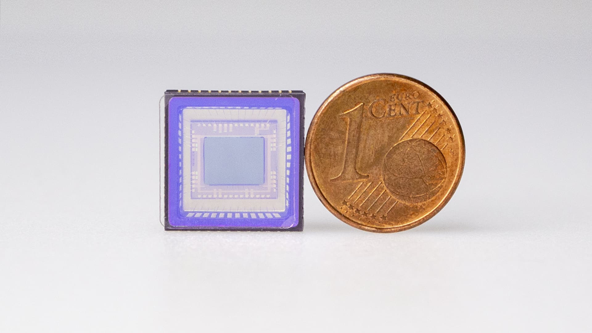
NIT controls and masters in-house all the design and manufacturing phases of its InGaAs focal plane arrays.

One of the critical steps is the 3D stacking of the photodiode array to the read-out circuit, for which NIT has developed a very innovative flip-chip process ensuring high yield and low cost of production.

The 3D stacking process is able to produce FPA’s from pitch of 7.5um to 15um, studies are underway to lower this limit.
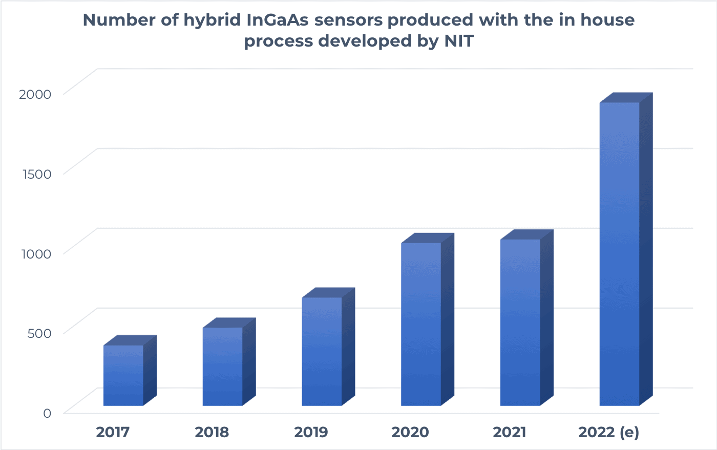
Number of hybrid InGaAs sensors produced with the in house process developed by NIT

Recent news

Join NIT at Embedded Vision Summit – EVS 2018

Join NIT at Embedded Vision Summit – EVS 2018

Join NIT at Embedded Vision Summit – EVS 2018 on May 21-24, 2018 in Santa Clara, California Embedded vision is now possible in all light conditions, even in outdoor scenes with high illumination, thanks to our HDR sensor NSC1602 and MAGIC mono board*. *Our mono board...

GATED IMAGING – Part 3

GATED IMAGING – Part 3

Learn about Gated imaging application in long-range imaging. Your specific region of interest will be accurately delimited thanks to our dedicated WiDy cameras. Gated Imaging - Long-range imaging - NIT Application note from NewImagingTechnologies

GATED IMAGING – Part 2

GATED IMAGING – Part 2

Learn about Gated Imaging and the ability to determine the distance between an object and the camera. Our dedicated WiDy cameras will lead to accurate tomographic reconstructions. Gated Imaging - Tomography - NIT Application note from NewImagingTechnologies